Support for simultaneous memory reading refers to the capability of a computing system's memory controller and underlying hardware architecture to service multiple, independent memory access requests from distinct processing units or threads concurrently. This contrasts with sequential memory access, where requests are processed one after another. Modern high-performance computing, including multi-core processors, GPUs, and specialized accelerators, necessitates this feature to maximize data throughput and minimize latency by allowing different computational entities to retrieve or store data from main memory without blocking each other. The efficiency of simultaneous memory reading is critically dependent on factors such as memory bus bandwidth, memory controller arbitration logic, memory channel configuration (e.g., dual, quad channel), and the underlying Random Access Memory (RAM) technology (e.g., DDR4, DDR5, HBM), which dictates the physical interface and signaling protocols.
Achieving effective simultaneous memory reading involves sophisticated hardware mechanisms and protocols. The memory controller acts as the central arbiter, managing the queue of read and write requests from various masters (CPUs, GPUs, I/O devices). Advanced controllers employ techniques like request reordering, bank and row interleaving, and command pipelining to exploit the inherent parallelism within DRAM modules. Interleaving, for instance, distributes data across multiple memory banks or ranks, allowing operations on different banks to proceed in parallel. The physical topology of the memory subsystem, including the number of memory channels, DIMM placement, and the use of memory buffers (like those found in high-bandwidth memory), plays a crucial role in determining the effective concurrency that can be achieved. Ensuring that memory access patterns are sufficiently distributed and that contention is minimized is paramount for realizing the performance benefits of simultaneous read operations.
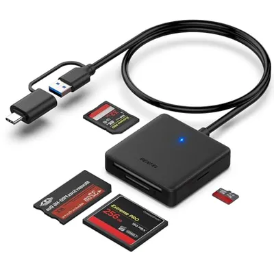
Mechanism of Action
The core mechanism for supporting simultaneous memory reading lies within the memory controller's design and the DRAM interface protocols. When multiple processing units (e.g., CPU cores, GPU compute units) issue memory read commands, these requests are typically funneled through a shared memory controller. The controller prioritizes, schedules, and arbitrates these requests to optimize throughput and latency. Key techniques include:
- Request Buffering and Queuing: The controller maintains queues for incoming read and write requests. Buffering allows requests to be held temporarily, enabling the controller to reorder them for efficiency.
- Arbitration Logic: Sophisticated algorithms determine the order in which requests are serviced. This logic considers factors such as request priority, memory bank availability, row buffer status, and fairness policies to prevent starvation of specific requesters.
- Bank and Rank Interleaving: DRAM is organized into banks and ranks. Accessing different banks or ranks concurrently allows for parallel operations. For example, if one bank is busy with a row precharge or active operation, the controller can immediately issue a command to a different, available bank.
- Command Pipelining: Modern memory interfaces (e.g., DDR SDRAM) support pipelining, where multiple commands (like Activate, Read, Precharge) can be in flight simultaneously, but in different stages of execution. This exploits the latency between DRAM operations.
- Channel Multiplexing: Systems with multiple memory channels can service requests independently on each channel, effectively multiplying the potential for simultaneous access if requests can be distributed across channels.
Industry Standards and Protocols
Support for simultaneous memory reading is intrinsically tied to the specifications of memory technologies and their associated bus protocols. Major standards dictate the signaling, timing, and command structures that enable concurrent operations:
Double Data Rate (DDR) SDRAM
DDR generations (DDR3, DDR4, DDR5) define the command/address bus and data bus protocols. These standards incorporate features that facilitate concurrency:
- On-Die Termination (ODT): Improves signal integrity, allowing for higher speeds and more reliable simultaneous transfers.
- Command/Address (CA) Bus Training: Ensures precise timing for commands and addresses, crucial for managing multiple simultaneous requests.
- DDR5 Enhancements: Introduces features like two independent 32-bit sub-channels per DIMM (effectively doubling the burst length and improving concurrency), improved power management, and advanced error correction codes (ECC) that can operate more efficiently with simultaneous accesses.
High Bandwidth Memory (HBM)
HBM, designed for applications requiring extremely high memory bandwidth (e.g., GPUs, AI accelerators), uses a different approach:
- Stacked DRAM Dies: Multiple DRAM dies are stacked vertically and connected via Through-Silicon Vias (TSVs).
- Wide Interface: Utilizes a very wide data interface (e.g., 1024 bits per stack) compared to traditional DIMMs.
- Multiple Logic Dies: Integrates logic dies that manage the interface, allowing for highly parallel access to the stacked DRAM. HBM's architecture is inherently designed for maximum parallelism and simultaneous access to data across its wide bus.
Architecture and Implementation
The architectural implementation of simultaneous memory reading involves both the memory controller integrated within the System-on-Chip (SoC) or CPU, and the physical memory subsystem.
Memory Controller
The memory controller is the central component responsible for managing traffic to and from DRAM. Its sophistication directly impacts the ability to perform simultaneous reads:
- Multi-Master Support: Controllers must be designed to handle requests from multiple bus masters (CPU cores, integrated GPUs, DMA engines, network interfaces).
- Quality of Service (QoS): Advanced controllers implement QoS mechanisms to prioritize certain types of traffic or applications, ensuring that critical read requests are serviced promptly, even under heavy load.
- Error Detection and Correction: ECC logic is integrated to detect and correct single-bit errors, essential for data integrity during high-volume, simultaneous transfers.
Memory Topology
The physical layout and configuration of the memory subsystem are critical:
- Memory Channels: Systems employ single, dual, quad, or even more memory channels. Each channel provides an independent data path to the memory modules, enabling parallel data transfer.
- DIMM Configuration: The number of DIMMs populated and their placement across channels (e.g., single-rank vs. dual-rank DIMMs) influences how effectively interleaving can be utilized. Dual-rank DIMMs present two independent sets of memory chips to the controller on a single module, providing an additional layer of parallelism.
- Interconnects: Technologies like Intel's Ultra Path Interconnect (UPI) or AMD's Infinity Fabric facilitate high-speed communication between CPUs and memory controllers, and between multiple CPU sockets, enabling efficient management of distributed memory resources.
Performance Metrics and Benchmarking
The effectiveness of simultaneous memory reading is quantified through various performance metrics:
- Memory Bandwidth: The maximum rate at which data can be read from or written to memory. This is a primary indicator of how much data can be transferred concurrently. Benchmarks like STREAM and AIDA64 Memory Benchmark measure sustained read and write bandwidth.
- Memory Latency: The time delay between initiating a memory read request and receiving the first piece of data. While simultaneous reading aims to increase throughput, minimizing latency for individual requests remains important, especially for latency-sensitive operations.
- IOPS (Input/Output Operations Per Second): Measures the number of read and write operations a storage system can perform per second. While more common for storage, high-frequency, small memory accesses can be analyzed in terms of IOPS to assess the controller's ability to handle many simultaneous small requests.
- Effective Throughput: The actual data transfer rate achieved under specific workloads, which accounts for overhead, contention, and non-ideal access patterns.
Benchmarking involves simulating various concurrent access patterns to stress the memory subsystem and measure its response. This includes testing with multiple threads simultaneously accessing different memory regions, as well as synthetic benchmarks that target specific aspects of memory controller performance.
Challenges and Limitations
Despite advancements, several challenges limit the efficacy of simultaneous memory reading:
- Memory Bandwidth Bottlenecks: Even with multiple channels and advanced RAM, the aggregate bandwidth can still become a bottleneck for extremely data-intensive workloads, particularly those involving large datasets or high-resolution streaming.
- Memory Controller Contention: While designed for concurrency, a single memory controller can still become overloaded if an excessive number of masters issue requests simultaneously, leading to arbitration delays and reduced performance.
- Access Pattern Dependencies: Performance is highly sensitive to the memory access patterns of the applications. Random or highly localized access patterns can lead to cache misses and increased demand on the main memory, exacerbating contention.
- Power Consumption and Heat Dissipation: Higher memory speeds and increased activity associated with simultaneous transfers contribute to higher power consumption and heat generation, which can necessitate thermal throttling and limit sustained performance.
- Signal Integrity: At very high frequencies and with complex bus topologies, maintaining signal integrity becomes challenging, potentially leading to errors that require retransmissions or data corruption.
Future Outlook
The trend towards greater parallelism in computing, driven by AI, machine learning, and big data analytics, will continue to increase the demand for highly efficient simultaneous memory reading capabilities. Future developments are expected to focus on:
- Increased Channel Count and Bandwidth: Integration of more memory channels and higher DDR standards (e.g., DDR6) will push raw bandwidth limits.
- Advanced Memory Architectures: Innovations like Compute Express Link (CXL) will enable more flexible memory pooling and coherency across heterogeneous computing platforms, requiring sophisticated memory controllers capable of managing distributed simultaneous access.
- On-chip Memory and Near-Memory Processing: Moving computation closer to or directly into memory (e.g., HBM with integrated logic) will reduce the need for data movement and optimize simultaneous access within localized processing units.
- AI-Optimized Memory Controllers: Future memory controllers may incorporate AI-driven predictive scheduling and resource allocation to proactively manage memory access patterns and mitigate contention before it impacts performance.
Ultimately, the evolution of simultaneous memory reading support is inseparable from the broader trends in processor architecture, memory technology, and interconnect standards, all converging to enable higher levels of data throughput and computational efficiency.