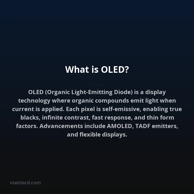
Organic Light-Emitting Diode (OLED) represents a display illumination technology where emissive electroluminescent organic compounds generate light when an electric current is applied. Unlike Liquid Crystal Displays (LCDs) which necessitate a separate backlight source (e.g., Cold Cathode Fluorescent Lamps or Light Emitting Diodes), each individual pixel in an OLED display functions as an independent light emitter. This intrinsic emissive nature enables OLED panels to achieve true blacks by completely deactivating pixels, resulting in superior contrast ratios, wider viewing angles, faster response times, and potentially thinner form factors compared to transmissive display technologies. The organic layers involved typically comprise a charge transport layer and a light-emitting layer, with specific molecular engineering dictating the color and efficiency of the emitted light.
The fundamental operational principle of an OLED involves the injection of charge carriers—holes from an anode and electrons from a cathode—into an organic semiconductor stack. These carriers migrate through organic layers under an applied electric field until they recombine within an emissive layer. This recombination event excites the organic molecules, which then relax to their ground state by emitting photons. The color of the emitted light is determined by the energy gap of the organic material used in the emissive layer. Advances in organic chemistry and materials science have led to the development of various OLED architectures, including small molecule OLEDs (SMOLEDs) and polymer OLEDs (PPOs), as well as different device structures like passive-matrix (PMOLED) and active-matrix (AMOLED) configurations, each offering distinct performance characteristics and manufacturing complexities.
Mechanism of Action
The operation of an OLED device relies on the principle of electroluminescence within organic semiconductor materials. The device structure typically consists of a substrate, an anode, an organic stack comprising hole injection layer (HIL), hole transport layer (HTL), emissive layer (EML), electron transport layer (ETL), and electron injection layer (EIL), and finally a cathode. When a forward bias voltage is applied across the anode and cathode, holes are injected from the anode (typically a transparent conductive oxide like Indium Tin Oxide, ITO) and electrons are injected from the cathode (often a low work function metal like Aluminum or Calcium). These charge carriers migrate towards each other through their respective transport layers. Upon reaching the emissive layer, holes and electrons recombine to form excitons—bound electron-hole pairs. The radiative decay of these excitons results in the emission of photons, with the photon energy (and thus the emitted light color) determined by the energy difference between the lowest unoccupied molecular orbital (LUMO) and the highest occupied molecular orbital (HOMO) of the emissive material. The efficiency of photon generation and emission is critically dependent on factors such as charge carrier mobility, exciton formation efficiency, photoluminescence quantum yield (PLQY) of the emissive material, and charge balance within the emissive layer.
OLED Device Architectures
Small Molecule OLEDs (SMOLEDs) vs. Polymer OLEDs (PPOs)
OLEDs can be broadly categorized based on the type of organic material used: small molecules or polymers. SMOLEDs employ small organic molecules that are typically vacuum-deposited onto the substrate. This vacuum thermal evaporation (VTE) process allows for precise control over layer thickness and composition, leading to highly efficient and stable devices. Examples of small molecules used include tris(8-hydroxyquinoline)aluminum (Alq3) for electron transport and green emission, and N,N′-di(naphthalen-1-yl)-N,N′-diphenyl-benzidine (NPB) for hole transport. PPOs, on the other hand, utilize conjugated polymers that can be processed from solution using techniques like spin-coating, inkjet printing, or roll-to-roll processing. This solution-processability offers potential advantages in terms of lower manufacturing costs and the ability to create large-area, flexible displays. However, PPOs often face challenges related to device stability, efficiency, and color purity compared to their vacuum-deposited small molecule counterparts.
Passive-Matrix vs. Active-Matrix OLEDs
Display driving schemes further differentiate OLEDs into passive-matrix (PMOLED) and active-matrix (AMOLED) configurations. In PMOLED displays, the pixels are arranged in a grid and are controlled by row and column electrodes. Each pixel receives current only when its corresponding row and column electrodes are simultaneously addressed. This simpler architecture is suitable for small, low-resolution displays but suffers from limited refresh rates and brightness as the number of pixels increases. AMOLED displays, conversely, employ a thin-film transistor (TFT) at each pixel. This TFT acts as a switch and a current regulator, allowing each pixel to be independently controlled and charged, thereby enabling higher resolutions, faster refresh rates, brighter images, and lower power consumption. The TFT backplane is typically fabricated using amorphous silicon (a-Si), low-temperature polysilicon (LTPS), or metal-oxide semiconductors like Indium Gallium Zinc Oxide (IGZO).
Materials and Physics
The performance of an OLED is intrinsically linked to the photophysical and electrochemical properties of the organic materials employed. Key material classes include hole-transporting materials (e.g., arylamines like NPB), electron-transporting materials (e.g., metal chelates like Alq3, or nitrogen-containing heterocycles), and emissive materials. Emissive materials can be further classified into fluorescent emitters, phosphorescent emitters, and, more recently, thermally activated delayed fluorescence (TADF) emitters. Fluorescent emitters utilize spin-allowed singlet excitons for light emission, achieving theoretical internal quantum efficiencies (IQE) of up to 25%. Phosphorescent emitters, based on heavy metal complexes (e.g., iridium or platinum), can harness both singlet and triplet excitons, leading to theoretical IQEs of up to 100%. TADF materials offer a pathway to achieve high efficiency without heavy metals by utilizing a small singlet-triplet energy gap that facilitates intersystem crossing (ISC) and reverse intersystem crossing (RISC) at room temperature, effectively harvesting triplet excitons via a delayed fluorescence mechanism.
| Parameter | Specification | Notes |
|---|---|---|
| Luminance | 100-1000 cd/m² (typical for consumer displays) | Can reach >10,000 cd/m² for HDR content |
| Contrast Ratio | Effectively infinite | Due to true black pixel generation |
| Response Time | < 1 microsecond | Significantly faster than LCD |
| Viewing Angle | Nearly 180 degrees | Minimal color shift or brightness degradation |
| Color Gamut | Rec. 2020, DCI-P3 coverage | Dependent on emitter materials |
| Power Consumption | Variable, pixel-dependent | Lower for dark content, higher for bright content |
| Lifespan (MTBF) | 20,000 - 100,000 hours | Varies by color and usage; blue emitters typically shortest lifespan |
History and Evolution
The foundational research in organic electroluminescence began in the 1960s with the work of Martin Pope and his colleagues at New York University, who demonstrated electroluminescence in anthracene crystals. However, the practical realization of efficient OLED devices is attributed to the pioneering work of Ching W. Tang and Steven Van Slyke at Eastman Kodak in 1987. They developed a multilayer device structure using vacuum-deposited small molecules, achieving significantly improved performance and laying the groundwork for subsequent advancements. Early commercialization efforts focused on PMOLED displays for small electronic devices like pagers and mobile phone sub-displays. The development of AMOLED technology, driven by the need for high-performance displays in smartphones and televisions, represented a major leap forward. Advancements in organic materials, particularly the discovery of phosphorescent emitters by the University of Southern California group (led by Mark Thompson) and subsequent commercialization by Universal Display Corporation (UDC), drastically improved device efficiency and lifespan, enabling widespread adoption in premium consumer electronics.
Applications
OLED technology has found widespread application across numerous electronic devices owing to its superior display characteristics. In the consumer electronics sector, OLED displays are prevalent in high-end smartphones, where their vibrant colors, deep blacks, and energy efficiency contribute to enhanced user experience. Televisions utilizing OLED panels are renowned for their cinematic picture quality, offering unparalleled contrast and HDR performance. The technology is also increasingly integrated into wearable devices like smartwatches and fitness trackers, benefiting from their thinness and low power consumption. Furthermore, OLEDs are utilized in monitors, increasingly targeting professional and gaming segments where fast response times and color accuracy are paramount. Beyond personal devices, OLEDs are employed in automotive dashboards and infotainment systems, digital signage, and specialized applications such as virtual reality (VR) headsets, where high refresh rates and minimal motion blur are critical for immersion.
Advantages and Disadvantages
The distinct advantages of OLED technology stem primarily from its self-emissive nature. Superior Contrast Ratio and Black Levels are achieved because individual pixels can be completely turned off, resulting in an infinite contrast ratio and true black representation, which is crucial for high dynamic range (HDR) content and overall image depth. Wide Viewing Angles ensure that image quality remains consistent even when viewed from oblique angles, with minimal color shift or brightness reduction. Fast Response Times, measured in microseconds, eliminate motion blur, making OLEDs ideal for fast-paced content like gaming and sports. The Thin and Flexible Form Factors are possible due to the absence of a backlight unit, allowing for the design of ultra-thin displays and even flexible or rollable screens. Additionally, OLEDs offer Energy Efficiency, particularly when displaying darker content, as only active pixels consume power.
However, OLED technology also presents certain disadvantages. Burn-in or Image Retention is a known issue, where static images displayed for extended periods can cause permanent degradation of organic materials, leading to ghosting. While modern OLEDs incorporate mitigation techniques like pixel shifting and screen savers, it remains a consideration for content with static elements. Color Shift and Brightness Degradation can occur over time, especially with certain color emitters (e.g., blue), impacting the longevity of color fidelity and peak brightness. The Higher Cost of Manufacturing, particularly for large-area panels, has historically made OLED displays more expensive than comparable LCD technologies. Finally, Susceptibility to Moisture and Oxygen necessitates robust encapsulation techniques to prevent degradation of the organic layers, adding to manufacturing complexity and cost.
Industry Standards and Performance Metrics
The performance and quality of OLED displays are often evaluated against established industry standards and key metrics. Color accuracy is frequently assessed using standards like the DCI-P3 color space, which is commonly used in digital cinema, and Rec. 2020, the ultra-high-definition television broadcast standard. Peak brightness, critical for HDR content, is measured in candelas per square meter (cd/m²). Contrast ratio, while theoretically infinite, is practically assessed by comparing the luminance of a full white screen to a full black screen. Response time is measured in milliseconds (ms) or microseconds (µs), indicating how quickly a pixel can transition between different color states. Viewing angles are quantified by the degree of off-axis viewing before significant luminance or color deviation occurs. Lifespan, often expressed as Mean Time Between Failures (MTBF), is a crucial metric for longevity, with different color sub-pixels having varying degradation rates. The International Electrotechnical Commission (IEC) and other bodies establish standards for display testing and performance, ensuring comparability and reliability.
Future Outlook
The trajectory of OLED technology indicates continued innovation in materials science, manufacturing processes, and application integration. Research is intensely focused on enhancing the efficiency and lifespan of blue emitters, which currently represent a bottleneck for achieving greater overall device longevity and energy savings. The development of novel TADF materials and improved phosphorescent emitters promises further gains in quantum efficiency. Advancements in solution-processing techniques, such as inkjet printing, are expected to drive down manufacturing costs and enable the production of even larger, more flexible, and transparent displays. The integration of OLEDs into flexible, foldable, and stretchable form factors will continue to expand their use in novel electronic devices and wearable technology. Furthermore, ongoing efforts aim to address and mitigate the risk of burn-in, making OLEDs more robust for a wider range of applications. The evolution towards higher resolution, increased brightness, and broader color gamuts will ensure OLEDs remain at the forefront of display technology.