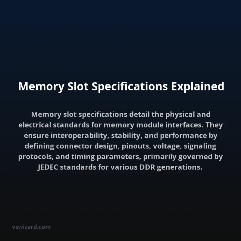
Memory slot specifications delineate the precise physical and electrical characteristics defining the interface between a memory module and a host system's motherboard. These specifications encompass a comprehensive set of parameters including physical dimensions, pin count and arrangement, signal voltage levels, data transfer protocols, timing requirements, power delivery specifications, and keying mechanisms to prevent incorrect module insertion. Adherence to these specifications is paramount for ensuring interoperability, stability, and optimal performance across diverse hardware configurations and memory module types, such as DDR (Double Data Rate) SDRAM (Synchronous Dynamic Random-Access Memory) generations (e.g., DDR3, DDR4, DDR5), LPDDR (Low Power Double Data Rate) variants, or specialized memory form factors. The engineering behind these specifications involves intricate considerations of signal integrity, thermal management, and electromagnetic compatibility to facilitate high-speed data exchange in computing systems ranging from consumer electronics to high-performance servers.
The standardization of memory slot specifications is driven by consortia like JEDEC (Joint Electron Device Engineering Council), which publishes definitive standards that govern memory module form factors (e.g., DIMM, SO-DIMM), pinouts, electrical signaling, and operational parameters. These standards ensure that memory modules manufactured by different vendors can be seamlessly integrated into motherboards designed by other manufacturers, fostering a robust and competitive ecosystem. Key aspects of these specifications include the physical connector design, which dictates the number of contacts and their positioning to align with the module's edge connector, and the electrical interface, which defines the data bus width, clock frequencies, voltage rails (e.g., VDD, VDDQ), and command/address signaling to facilitate synchronous data transfers. Furthermore, specifications address physical keying notches on the memory module to prevent installation in incompatible slots, thereby safeguarding both the module and the system from damage.
Physical Form Factor and Connector Design
DIMM (Dual In-line Memory Module)
The DIMM form factor is prevalent in desktop computers and servers. Specifications dictate the number of pins (e.g., 240 pins for DDR3/DDR4 UDIMM, 288 pins for DDR4/DDR5 RDIMM/LRDIMM), module dimensions (length, width, height), and the specific layout of electrical contacts. The physical keying notch is crucial, positioned to align with a corresponding key on the motherboard slot, preventing insertion of modules designed for different voltage standards or generations. For instance, DDR3, DDR4, and DDR5 DIMMs have keying notches located at different positions to ensure mechanical and electrical compatibility is maintained.
SO-DIMM (Small Outline Dual In-line Memory Module)
Primarily used in laptops, small form-factor PCs, and some embedded systems, SO-DIMMs are physically smaller than DIMMs. Specifications define their reduced pin count (e.g., 200 pins for DDR2, 204 pins for DDR3, 260 pins for DDR4, 262 pins for DDR5) and smaller physical dimensions while maintaining similar electrical interface principles to their larger DIMM counterparts.
Electrical Interface and Signaling
Voltage Standards
Memory slot specifications precisely define the operating voltages required for the memory modules. These include VDD (power supply voltage for the memory array and I/O buffers), VDDQ (I/O power supply voltage), and VPP (programming voltage for specific functionalities, less common in standard RAM). For example, DDR3 operates at 1.5V, DDR4 at 1.2V, and DDR5 at 1.1V, with variations for low-power variants. The slot must be capable of delivering these voltages stably.
Data Transfer Protocols and Speeds
Specifications detail the synchronous data transfer protocols, such as DDR, DDR2, DDR3, DDR4, and DDR5. This involves defining clock frequencies, burst lengths, prefetch capabilities, and command/address signaling timing. The bandwidth of the memory subsystem is directly determined by the data transfer rate (MT/s or MHz) and the bus width (e.g., 64-bit for standard DIMMs).
Timing Parameters
JEDEC standards meticulously define critical timing parameters, including CAS Latency (CL), Row Address to Column Address Delay (tRCD), Row Precharge Time (tRP), and Active to Precharge Delay (tRAS). These parameters dictate the minimum time delays between various memory operations and are crucial for data integrity and system stability at specified clock speeds.
Industry Standards and Organizations
The standardization body JEDEC plays a pivotal role. Its JESD (JEDEC Standard) publications, such as JESD79 (DDR SDRAM) and JESD209 (LPDDR SDRAM), provide the foundational specifications for memory modules and their interfaces. These documents are comprehensive, covering mechanical, electrical, and timing aspects, ensuring a baseline level of compatibility and performance.
Implementation and Practical Considerations
Motherboard Design
Motherboard manufacturers must adhere to JEDEC specifications when designing memory slots. This includes the physical layout of the connector, the routing of high-speed signal traces to minimize impedance discontinuities and crosstalk, the provision of stable power delivery through voltage regulators, and the implementation of appropriate termination schemes. The slot's physical construction also affects durability and ease of use.
Module Compatibility
Understanding memory slot specifications is critical for end-users when selecting compatible memory modules for their systems. Using modules that do not meet the motherboard's slot specifications can result in the system failing to boot, data corruption, or even permanent hardware damage due to incompatible voltage levels or signaling protocols.
Performance Metrics
Key performance metrics related to memory slot specifications include:
- Bandwidth: The maximum rate at which data can be transferred, calculated as (Memory Clock Speed) × (Bus Width / 8 bits/byte) × (DDR factor).
- Latency: The time delay between requesting data and its availability, influenced by timing parameters like CL.
- Throughput: The actual sustained data transfer rate achievable in real-world applications.
Comparative Table: DDR SDRAM Generations
| Specification | DDR3 | DDR4 | DDR5 |
|---|---|---|---|
| Standard Voltage (VDD/VDDQ) | 1.5V / 1.5V | 1.2V / 1.2V | 1.1V / 1.1V |
| Module Type | DIMM / SO-DIMM | DIMM / SO-DIMM | DIMM / SO-DIMM |
| Pin Count (DIMM) | 240 | 288 | 288 |
| Pin Count (SO-DIMM) | 204 | 260 | 262 |
| Prefetch | 8n | 8n | 16n (32n effective) |
| Data Rate (MT/s) | 800 - 2133 | 1600 - 3200+ | 4800 - 8400+ |
| Keying Notch Position | Different from DDR4/DDR5 | Different from DDR3/DDR5 | Different from DDR3/DDR4 |
| On-module PMIC | No | No | Yes |
Evolution and Future Trends
Memory slot specifications have evolved continuously, driven by the demand for higher bandwidth and lower power consumption. Each generation (DDR3 to DDR5, LPDDR variants) introduces improvements in signaling integrity, efficiency, and density. Future trends suggest further increases in data rates, potential architectural changes like on-module voltage regulation becoming standard (as seen in DDR5), and advancements in signal processing to overcome physical limitations of connectors and traces. The integration of higher performance memory directly onto processor packages (e.g., HBM - High Bandwidth Memory) also represents a parallel evolutionary path, diverging from traditional DIMM-based slot specifications but addressing similar performance imperatives.
FAQ
What is the primary function of memory slot specifications?
The primary function of memory slot specifications is to define the physical and electrical interface standards between a memory module and a host system's motherboard. These standards ensure that memory modules are mechanically compatible (preventing incorrect insertion), electrically compatible (correct voltage and signaling), and perform according to defined timing and speed parameters, thereby guaranteeing interoperability and system stability.
Who defines memory slot specifications?
Memory slot specifications are primarily defined by industry standards organizations, most notably JEDEC (Joint Electron Device Engineering Council). JEDEC develops and publishes detailed technical standards (e.g., JESD79 for DDR SDRAM) that govern the design and performance characteristics of memory modules and their corresponding slots, ensuring a consistent ecosystem.
How do memory slot specifications ensure compatibility?
Compatibility is ensured through multiple facets of the specifications: physical keying notches on the module and slot prevent installation in incompatible sockets; defined pinouts dictate the function of each electrical contact; standardized voltage levels prevent electrical damage; and precise timing parameters ensure synchronous operation between the memory controller and the module. Adherence to these comprehensive specifications allows modules from different manufacturers to function in systems built by other vendors.
What are the key differences between DDR4 and DDR5 slot specifications?
Key differences include a lower standard operating voltage for DDR5 (1.1V vs. 1.2V for DDR4), increased burst length (BL16 vs. BL8), a higher data transfer rate capability (starting at 4800 MT/s for DDR5 vs. 1600 MT/s for DDR4), and the integration of Power Management Integrated Circuits (PMICs) directly onto DDR5 modules, whereas DDR4 relies on the motherboard for power management. Additionally, DDR5 features dual independent 32-bit sub-channels per module, enhancing efficiency.
Can a DDR4 memory module be used in a DDR5 slot?
No, a DDR4 memory module cannot be used in a DDR5 slot, and vice versa. While both use 288 pins for DIMMs, the physical keying notch is located in a different position for DDR5 compared to DDR4. This mechanical difference, along with different electrical signaling and voltage requirements, prevents incompatible module insertion and ensures that only correctly specified modules are installed, protecting the hardware.