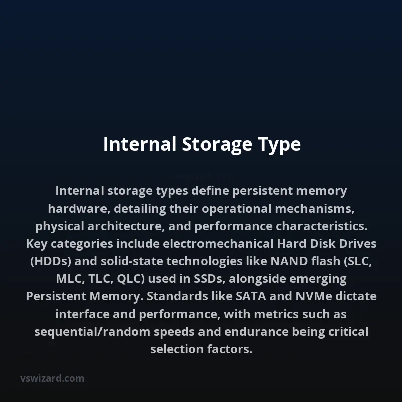
Internal storage type refers to the fundamental technological classification of persistent memory components integrated within a computing device, dictating their operational principles, data retention mechanisms, performance characteristics, and physical architecture. This classification transcends mere form factor or capacity, delving into the underlying semiconductor physics and engineering that enable the non-volatile storage of digital information. Key differentiators include the method of data encoding (e.g., charge trapping, magnetic orientation, phase transition), the mechanism of data access (sequential versus random), power requirements for operation and retention, and endurance limitations governed by physical wear or charge leakage phenomena. Understanding internal storage type is paramount for optimizing system performance, managing data integrity, and selecting appropriate hardware for diverse computational workloads and environmental conditions.
The categorization of internal storage types is broadly bifurcated into solid-state technologies, characterized by the absence of moving mechanical parts, and legacy electromechanical systems. Solid-state drives (SSDs) predominantly utilize NAND flash memory, wherein data is stored by trapping electrical charge in floating gates within semiconductor cells, offering high read/write speeds and low latency. In contrast, hard disk drives (HDDs) employ magnetic platters that are physically rotated and accessed by read/write heads, providing higher areal density and lower cost per gigabyte but with significantly slower access times and susceptibility to mechanical shock. Emerging technologies like Persistent Memory (PMEM), which blurs the lines between DRAM and NAND flash, further refine this landscape by offering byte-addressability, DRAM-like speeds, and non-volatility, fundamentally altering system architecture paradigms.
NAND Flash Memory Architectures
NAND flash memory, the predominant technology in Solid-State Drives (SSDs), is characterized by its array architecture and the method of charge storage. It is organized into blocks, which are further subdivided into pages. Data is written and read at the page level, but erased at the block level. This asymmetry is a fundamental aspect of its operation. The basic unit of storage is the memory cell, which typically stores one or more bits of data. The primary types of NAND flash are distinguished by the number of bits stored per cell:
Single-Level Cell (SLC)
SLC NAND flash stores one bit of data per cell. This is achieved by using two distinct voltage levels to represent a '0' or a '1'. The larger voltage margin between these states leads to higher reliability, superior endurance (rated in Program/Erase cycles, typically 50,000-100,000), and faster read/write speeds compared to multi-level cell technologies. Its primary drawback is lower data density, resulting in higher cost per gigabyte. SLC is often reserved for enterprise-grade applications demanding maximum performance and longevity.
Multi-Level Cell (MLC)
MLC NAND flash stores two bits of data per cell by employing four distinct voltage levels. This increased density comes at the expense of reduced endurance (typically 3,000-10,000 P/E cycles) and slightly slower performance due to the increased complexity in reading and programming the cell. Reliability is also reduced due to smaller voltage margins.
Triple-Level Cell (TLC)
TLC NAND flash stores three bits of data per cell, requiring eight distinct voltage levels. This offers even higher storage density and lower cost, making it prevalent in consumer-grade SSDs. However, it further compromises endurance (typically 500-3,000 P/E cycles) and performance, necessitating sophisticated error correction code (ECC) and wear-leveling algorithms to manage its inherent limitations.
Quad-Level Cell (QLC)
QLC NAND flash stores four bits per cell, utilizing sixteen voltage levels. This maximizes density and minimizes cost, but significantly reduces endurance (typically 100-1,000 P/E cycles) and write performance. QLC is generally suitable for read-intensive workloads or archival storage where write endurance is not a primary concern.
Hard Disk Drive (HDD) Technology
Hard Disk Drives represent an electromechanical storage paradigm utilizing magnetic storage principles. Data is encoded as magnetic orientations on the surface of rotating platters, which are coated with a magnetic material. A read/write head, suspended on a precise actuator arm, moves across the platter surface to access specific data sectors.
Platter Technology and Magnetism
Platters are typically constructed from aluminum or glass-ceramic substrates, coated with multiple thin layers, including a metallic magnetic layer where data is stored. Data is organized into concentric tracks, and each track is divided into sectors. The encoding of bits relies on altering the magnetic polarity of tiny regions on the platter surface. Perpendicular Magnetic Recording (PMR) and Shingled Magnetic Recording (SMR) are common techniques used to increase data density. PMR aligns magnetic bits perpendicular to the platter surface, while SMR overlaps tracks to fit more data, albeit with write performance implications.
Actuator and Read/Write Heads
The actuator arm, controlled by a voice coil motor, positions the read/write heads over the correct track. Modern HDDs employ multiple platters and read/write heads, enabling parallel access to data and increasing capacity. The read/write heads float microscopically above the platter surface on a cushion of air generated by the platter's rotation, preventing physical contact and wear.
Persistent Memory (PMEM)
Persistent Memory technologies, such as Intel Optane™ DC Persistent Memory, represent a significant shift by offering characteristics of both DRAM and NAND flash. They provide byte-addressability and high performance comparable to DRAM, coupled with non-volatility, meaning data is retained when power is removed. This allows for larger memory footprints and new application architectures that can directly access persistent data without the latency overhead of traditional storage I/O.
Storage Class Memory (SCM)
PMEM often falls under the broader category of Storage Class Memory (SCM), a tier of memory designed to bridge the performance gap between DRAM and NAND flash. It typically utilizes technologies like 3D XPoint™ to achieve its unique properties.
Industry Standards and Interfaces
The functionality and interoperability of internal storage types are governed by several industry standards and interface protocols:
SATA (Serial ATA)
Serial ATA is a standard interface for connecting storage devices, primarily HDDs and SATA SSDs, to the motherboard. It offers sequential data transfer rates that have evolved over several generations (SATA I, II, III), with SATA III reaching up to 6 Gb/s (approximately 600 MB/s).
NVMe (Non-Volatile Memory Express)
NVMe is a protocol and interface designed specifically for accessing NAND flash-based storage media attached via the PCI Express (PCIe) bus. It offers significantly higher performance than SATA by enabling greater parallelism, lower latency, and support for a much larger number of I/O commands. PCIe generations (e.g., PCIe 3.0, 4.0, 5.0) dictate the maximum bandwidth available to NVMe SSDs.
UFS (Universal Flash Storage)
Universal Flash Storage is a standard interface primarily used in mobile devices and some embedded systems. It leverages a command-queue interface similar to NVMe but is optimized for the form factor and power constraints of mobile platforms. UFS offers high-speed data transfer and multitasking capabilities.
Performance Metrics and Considerations
Evaluating internal storage performance involves several key metrics:
Sequential Read/Write Speeds
Measure the speed at which large, contiguous blocks of data can be transferred. Crucial for tasks like video editing, large file transfers, and loading large game assets.
Random Read/Write Speeds (IOPS)
Measure the speed at which small, non-contiguous data blocks are accessed. Expressed in Input/Output Operations Per Second (IOPS), this is critical for operating system responsiveness, application loading, and multitasking.
Latency
The time delay between a request for data and the actual delivery of that data. Lower latency is essential for applications sensitive to delays.
Endurance
The total amount of data that can be written to the storage device over its lifetime before it is expected to fail. Measured in Terabytes Written (TBW) or Drive Writes Per Day (DWPD). This is particularly relevant for NAND flash-based storage.
Form Factors
Internal storage devices come in various physical sizes and connector types:
- 2.5-inch: Common for SATA SSDs and HDDs, designed to fit in laptop drive bays.
- M.2: A compact form factor for SSDs, often connecting via NVMe/PCIe or SATA.
- U.2: A 2.5-inch form factor designed for enterprise NVMe SSDs, offering hot-swap capabilities.
- Add-in Card (AIC): PCIe expansion cards populated with storage controllers and NAND flash.
Comparative Analysis Table
The following table summarizes key characteristics of common internal storage types:
| Storage Type | Primary Technology | Interface | Typical Max Sequential Read | Typical Max Sequential Write | Typical Endurance (P/E Cycles) | Cost per GB (Relative) | Latency |
|---|---|---|---|---|---|---|---|
| HDD | Magnetic Platters | SATA | 250 MB/s | 200 MB/s | N/A (Mechanical Wear) | Low | Moderate to High |
| SATA SSD (TLC) | NAND Flash (TLC) | SATA III | 550 MB/s | 520 MB/s | 500-3,000 | Medium | Low |
| NVMe SSD (TLC) | NAND Flash (TLC) | PCIe 3.0 x4 | 3,500 MB/s | 3,000 MB/s | 500-3,000 | Medium | Very Low |
| NVMe SSD (QLC) | NAND Flash (QLC) | PCIe 4.0 x4 | 7,000 MB/s | 6,500 MB/s | 100-1,000 | Low | Very Low |
| Enterprise NVMe SSD (SLC/MLC) | NAND Flash (SLC/MLC) | PCIe 4.0 x4 | 7,000+ MB/s | 6,000+ MB/s | 50,000-100,000 (SLC), 3,000-10,000 (MLC) | High | Very Low |
| Persistent Memory (e.g., Optane) | 3D XPoint™ | DDR4 (via specific controller) | ~4,500 MB/s | ~3,000 MB/s | Very High (e.g., 1.5M P/E cycles) | Very High | Extremely Low |
Conclusion on Internal Storage Types
The evolution and diversification of internal storage types reflect a continuous engineering drive towards higher capacities, increased performance, and improved cost-efficiency. From the mechanical precision of HDDs to the semiconductor physics governing NAND flash and the emerging paradigms of Persistent Memory, each type occupies a distinct niche defined by its operational characteristics. The selection of an appropriate internal storage type is a critical design decision, directly impacting system responsiveness, data throughput, power consumption, and total cost of ownership. As technology progresses, the lines between traditional storage and memory tiers will likely continue to blur, enabling more sophisticated computing architectures and unlocking new possibilities in data-intensive applications.