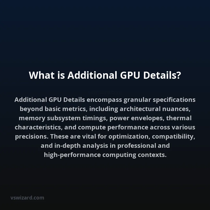
Additional GPU Details refer to a comprehensive set of parameters and metrics that extend beyond the foundational specifications of a Graphics Processing Unit (GPU). These encompass, but are not limited to, intricate architectural nuances, thermal dissipation characteristics, power consumption envelopes under varied operational loads, memory sub-system timings and configurations, interconnect bandwidths (e.g., PCIe generation and lane count), and specific shader unit functionalities. They are crucial for in-depth performance analysis, compatibility assessments, power management strategies, and the development of specialized software or hardware accelerators.
The extraction and interpretation of these additional details are vital for advanced users, system integrators, benchmarking professionals, and researchers aiming to optimize computational workflows or understand the nuanced performance differentials between GPU models. This information often resides within hardware monitoring tools, driver control panels, system information utilities, and vendor-specific diagnostic software, providing a granular view of the GPU's operational state and its underlying engineering design principles. Understanding these specifics facilitates fine-tuning for specific applications, from high-performance computing (HPC) and scientific simulations to professional content creation and complex AI model training.
GPU Architecture and Core Components
Shader Units and Execution Cores
Modern GPUs employ a highly parallel architecture. The core processing units are typically referred to as shader units, streaming multiprocessors (SMs) for NVIDIA, or compute units (CUs) for AMD. These units house numerous Arithmetic Logic Units (ALUs) capable of executing floating-point and integer operations. Additional details include the number of ALUs per SM/CU, clock speeds of these cores, and the specific instruction sets supported (e.g., FP32, FP16, INT8, TF32, BF16). Architectural specifics also cover cache hierarchies (L1, L2), register file sizes, and the scheduling mechanisms employed for work-group dispatch.
Memory Subsystem
The GPU's memory subsystem is a critical determinant of performance. Beyond standard VRAM capacity (e.g., GDDR6, HBM2e) and effective bandwidth, additional details include memory bus width (e.g., 256-bit, 384-bit), memory clock speed, memory latency, and the number of memory controllers. For High Bandwidth Memory (HBM), details such as the number of stacks, dies per stack, and interposer technology are significant. Error Correction Code (ECC) support is another vital specification for data integrity in critical applications.
Interconnects and Display Controllers
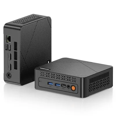
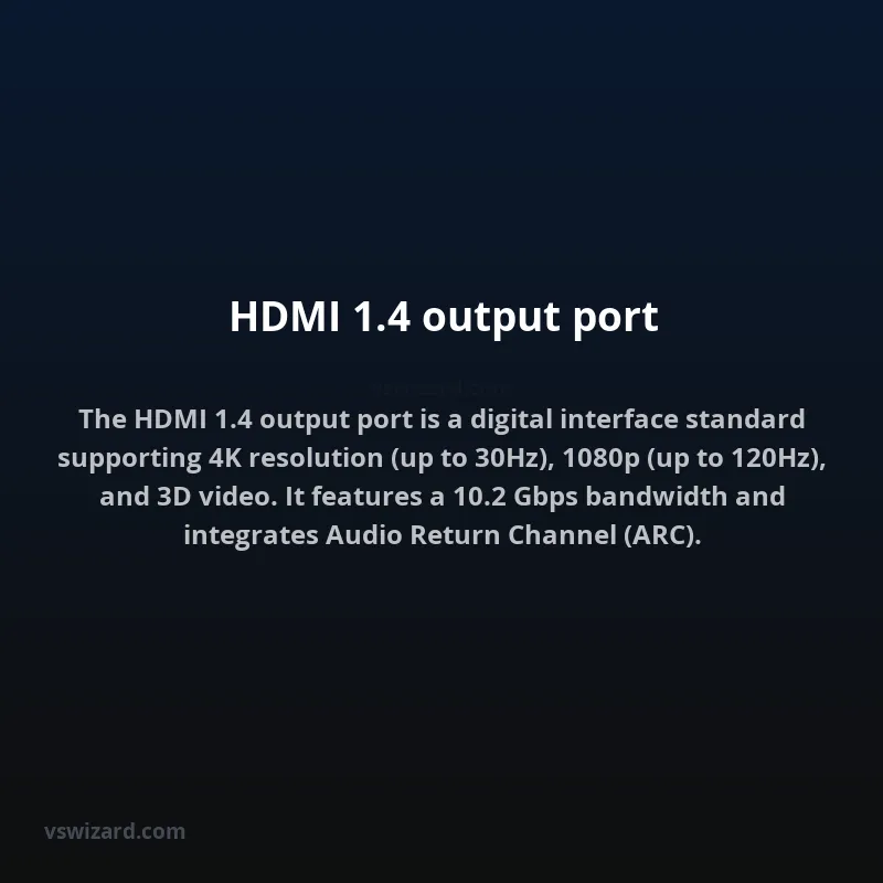
The interface to the rest of the system is typically PCI Express (PCIe). Additional details here include the PCIe generation (e.g., PCIe 4.0, PCIe 5.0) and the number of lanes utilized (e.g., x16). For multi-GPU configurations, technologies like NVIDIA NVLink or AMD Infinity Fabric provide higher bandwidth interconnects, and their specifications (bandwidth, topology) are crucial. Display controller details, including the number and types of display outputs (e.g., DisplayPort 1.4a, HDMI 2.1) and support for technologies like G-Sync or FreeSync, are also considered additional specifications.
Performance Metrics and Power Characteristics
Computational Throughput
Beyond raw theoretical peak performance (e.g., TFLOPS), additional details involve actual measured throughput in specific workloads. This includes single-precision (FP32), double-precision (FP64), half-precision (FP16), and mixed-precision (e.g., TF32, BF16) performance. Tensor Core performance for AI workloads and Ray Tracing (RT) core performance for realistic rendering are increasingly important metrics.
Thermal Design Power (TDP) and Power Efficiency
TDP is a fundamental specification, but additional details encompass actual power consumption under various loads (idle, gaming, rendering, compute). Power efficiency metrics, such as performance per watt or TFLOPS per watt, are crucial for high-density deployments and mobile devices. Understanding the power delivery subsystem, including VRM design and auxiliary power connectors, is also part of these additional details.
Thermals and Acoustics
GPU cooling solutions are diverse. Additional details include the specific heatsink design (e.g., vapor chamber, number of heat pipes), fan configuration (e.g., axial, blower, number of fans), and thermal throttling behavior. Acoustic performance, measured in decibels (dBA) under load, is also a key consideration for user experience.
Industry Standards and APIs
Graphics APIs
GPUs adhere to graphics and compute APIs. Primary examples include DirectX (versions 11, 12 Ultimate), Vulkan, and Metal (for Apple platforms). Support for specific features within these APIs, such as Ray Tracing extensions or Mesh Shading, constitutes additional detail.
Compute APIs
For general-purpose computing on GPUs (GPGPU), CUDA (NVIDIA) and OpenCL/ROCm (AMD/Open Standard) are paramount. Detailed specifications involve the version support, supported data types, and the efficiency of their respective runtimes and libraries.
Applications and Use Cases
Gaming and Professional Visualization
In gaming, additional details help in selecting GPUs that meet specific performance targets for resolution, frame rate, and graphical fidelity. For professional visualization (CAD, DCC), features like certified drivers, ECC memory support, and specific viewport performance metrics are critical.
High-Performance Computing (HPC) and AI
For HPC and AI, the focus shifts to compute throughput (FP64, FP16, INT8), memory bandwidth, interconnect capabilities for distributed training, and specialized hardware accelerators (e.g., Tensor Cores). Power efficiency and thermal management are also paramount in large-scale deployments.
Technical Specifications Table
| Specification Category | Detail | Example Metrics | Relevance |
|---|---|---|---|
| Architecture | Shader Core Count (SMs/CUs) | 100 SMs / 64 CUs | Parallel processing capacity |
| Architecture | Execution Units per SM/CU | 128 FP32 Cores per SM | Fine-grained computational power |
| Memory | Memory Bandwidth | 768 GB/s | Data transfer rate to VRAM |
| Memory | Memory Latency | ~50 ns | Time to access VRAM |
| Interconnect | PCIe Generation & Lanes | PCIe 4.0 x16 | System data transfer interface |
| Interconnect | NVLink/Infinity Fabric Bandwidth | 100 GB/s (bidirectional) | Multi-GPU communication speed |
| Power | Peak Power Draw | 350 W | Maximum operational power consumption |
| Power | Idle Power Draw | 20 W | Power consumption when inactive |
| Thermals | Typical Operating Temperature | 70-75°C under load | GPU stability and longevity |
| Compute | TF32 Performance | 150 TFLOPS | AI training throughput |
| Compute | FP64 Performance | 20 TFLOPS | Scientific simulation throughput |
Future Trends and Considerations
The continuous evolution of GPU architectures introduces more complex and specialized details. Emerging trends include increased integration of AI accelerators, more sophisticated power management techniques for improved efficiency, and advancements in memory technologies offering higher bandwidth and lower latency. Heterogeneous computing, where CPUs and GPUs collaborate more seamlessly, will likely lead to new metrics and considerations regarding inter-processor communication and data coherency. Furthermore, the development of specialized GPUs for areas like cryptocurrency mining or edge AI will necessitate a focus on specific architectural optimizations and efficiency metrics tailored to those domains.